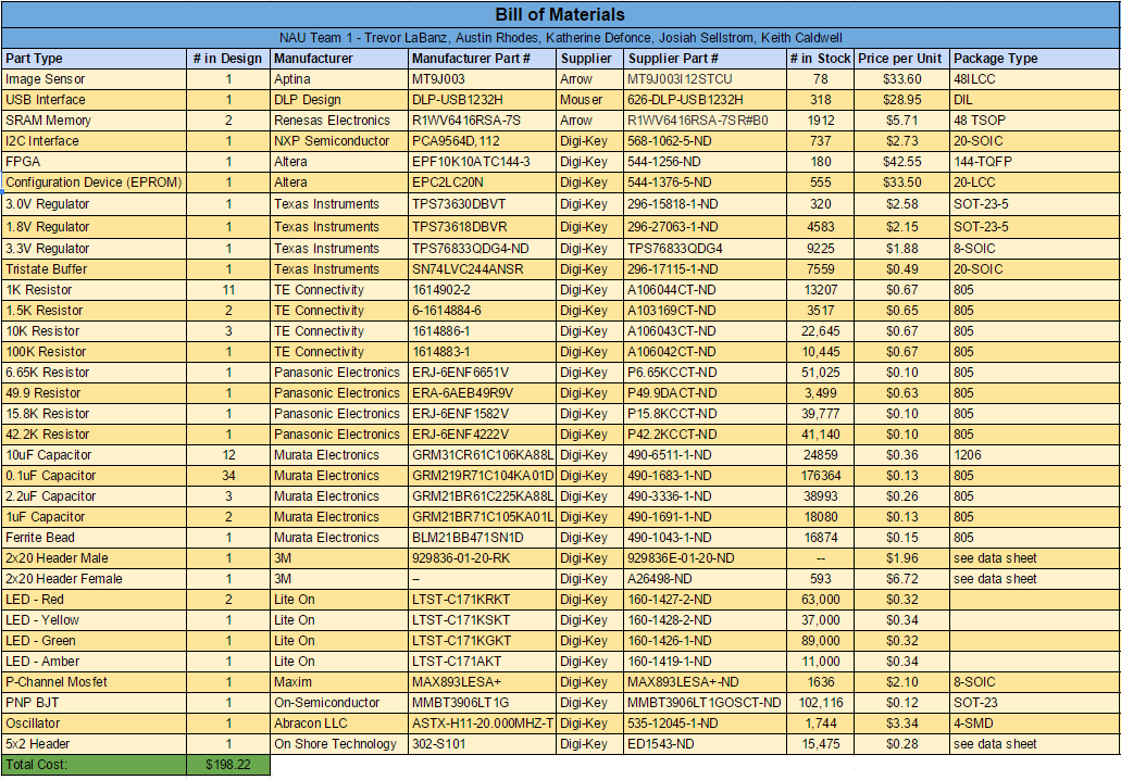
Summary

This "Detailed Design Phase" began at the beginning of the Spring 2015 semester (January 12th, 2015), and concluded at the midpoint in the semester (March 23rd, 2015). This phase started following the Concept Generation phase, where many of the parts were researched, and is the most technical portion of the design process. This design phase is succeeded by the Testing and Optimization phase, which will be the final stage in this project.

Altera Hardware Description Language (AHDL)

In order to control the memory, the image sensor, I2C bus, and USB interface, a control system had to be implemented. This control system was implemented using a Field Programmable Gate Array (FPGA) using AHDL. Through the AHDL, the image sensor is able to pass its data to SRAM banks to be temporarily stored until it can be passed through the USB interface. In addition to the memory control, the AHDL also controls the I2C commands that get issued from the user through MATLAB to control different aspects of the imager such as gain.

Bill of Materials

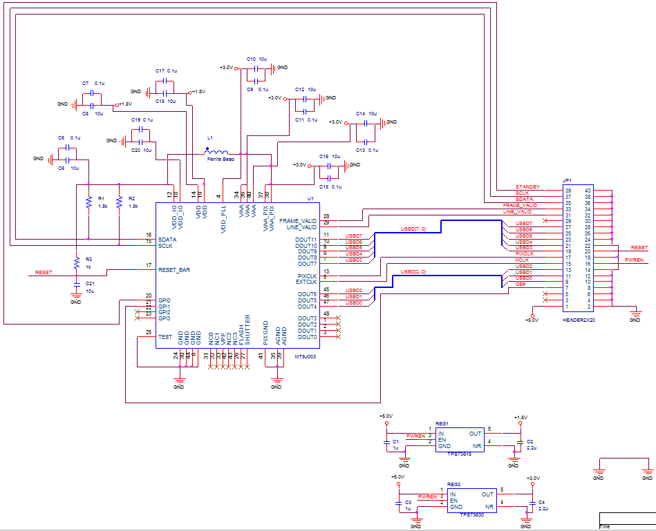
During the detailed design phase, in order to continue progressing in the project, more parts needed to be purchased. Some of the parts for this design were purchased previously, and can be seen on the Concept Generation Phase page on this website.


Below is the finalized Bill of Materials, which encompasses all elements necessary for building this project. Many of the elements were not included for the previous Bill of Materials, simply because small components such as resistors and capacitors were not yet determined at that time. A few of the components have been altered from the previous B.O.M., such as the 3.3 Volt regulator, due to the ever-changing requirements of this project. The combined cost for all of the parts in the Bill of Materials comes to $198.22. This total does not, however, include the cost of PCB fabrication. With the cost of PCB fabrication, the total is still underneath the goal budgetary price of $300.00 per fabricated complete part.

Complete BOM
Schematic Design

In order to begin the design process, a schematic had to be created using OrCad Schematic Capture. The schematics contained two separate sheets, one for the sensor board that contains the image sensor that will measure the radiation and supporting circuitry, and one for the control board that contains the FPGA, SRAM, I2C, Tristate buffers, and other circuitry that controls the operation of the design overall. These two sheets correspond to two separate PCBs that will be connected via a header that communicate the signals between the two. The individual parts for the schematics had to be created by hand or imported from OrCad's part library. To create the parts, the pins had to be numbered and labeled in accordance with their respective datasheets. The design implements three separate power supplies to regulate the voltage supplied by the USB. In addition to the voltage regulators, decoupling capacitors were required to clean the power supplied to many of the components. When the parts were all placed, connections were made between the various components to create a preliminary routing idea for the PCB layout. In addition, these connections were transferred to OrCad Allegro PCB so that connections could be suggested during PCB layout.

Sensor Board Schematic

Sensor Board Schematic

Printed Circuit Board (PCB) Design

In order to be able to actualize the schematics shown in the section to the left, the group needed to design a PCB, using OrCad Allegro PCB Editor. This Printed Circuit Board utilizes many different layers including: a layer for power, a layer for ground, and multiple signal layers. These signal layers are where “traces” are run, which are copper lines that connect each of the many components that exist on the board. For example, in this design the many different addressing lines needed to be connected not only to both memory (RAM) chips, but also to the Field Programmable Gate Array (FPGA), the USB Adapter, and the Tri-State buffer. The most important element on the PCB is the FPGA, which controls all of the signals that go in between the different components, and also controls the data flow to and from the USB Adapter. This is how the device accepts new parameters from the computer interface, and also how the device outputs the images to the MATLAB window. In order to conserve space, and also to make the design easier, the group decided to have components on both the top and bottom of the Printed Circuit Board. This allows for there to be more room for the parts as well as the routes that connect them.

Top Layer PCB

PCB Top Layer

MATLAB Graphical User Interface (GUI) Development
GUI

A GUI was designed for the control side of the design. This was done for several reasons:

  • Ease of use
  • The design is intended to be as easy to use as possible for users of all backgrounds. By removing the user from the MATLAB code itself, the ease of use of the device will be greatly increased.
  • Reliability
  • To ensure compatibility with many versions of MATLAB, the controlling code can be run independent of the GUI. Because many of GUI elements rely on the current MATLAB version there is the possibility that the end user will need access the underlying code without the GUI, this has been taken into account.
  • Features
The final GUI incorporates many extra features such as the ability to generate an AVI video of the captured images. In addition, there are options that give the user the ability to control many aspects of the sensor. The features include:
  1. Number of Frames: The number of images taken for processing.
  2. Movie Frame Rate: Frame rate that the AVI video using the images is generated at.
  3. Display Format: Whether to display the captured images in color or grayscale.
  4. Save currently displayed image
  5. Save all images
  6. Print currently displayed image
  7. Zoom and pan on images
  8. Close communication ports (required in case of errors where MATLAB leaves the ports open)