Project Overview | System Overview | Significant Milestones | Tools used During Design | Development and Testing | Problems and Tradeoffs
Development and Testing:
Below are the systems specifications of our modifed new system:
Old system Project Requirements:
Frequency Range: 208MHz-304MHz
Step size: 8.33kHz
Reference Frequency: 16MHz
PLL RF Output Impedance: 50Ω
PLL RF Output Power: +17dBm ± 0.5dBm
Digital Lock Detect Signal
Fractional N Divider
RS-232 Interface
PCBNew System Requirements:
Frequency Range: 1kHz-300kHz
Step size: 625Hz
Reference Frequency: 10kHz
Fractional N Divider
Digital Lock Detect Signal
Digital Interface: Basic stamp
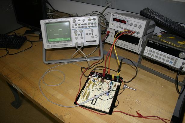
The system is still in the process of being integrated:
Running system test on componts of the PLL.
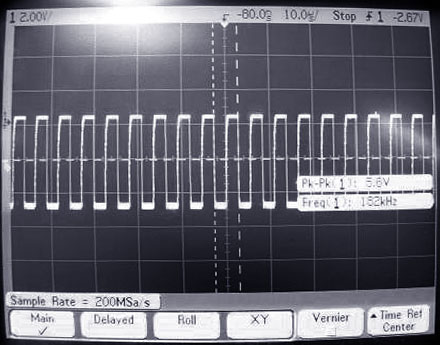
VCO output: test output at 182KHz.
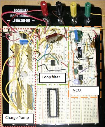
Charge pump, low pass filter, and VCO curcuits
Below are componets we build for the operation of the PLL:
Voltage Inverter:
The two voltage inverters basically take in a voltage on either the positive or negative rail and outputs a voltage on the opposing rail.
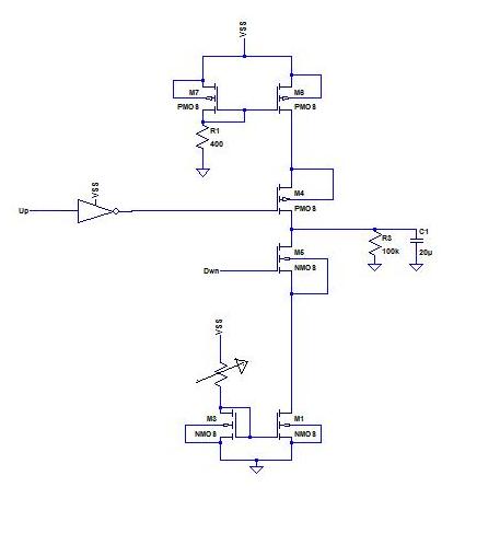
Charge pump:
This circuits consists of two MOSFET switches and two current mirrors. It responsible for increasing, decreasing, and maintaining the voltage on the low pass filter.
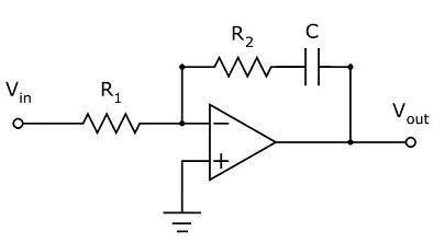
Low Pass filter:
This circuit acts as an integrator for the signal coming out of the control pump, as well as, helping to reduce spurious noise.
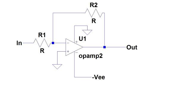
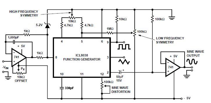
Linear Voltage Controlled Oscillator:
Our VCO consists of a ICL8038 function generator IC and two op amps. The VCO is linear, but requires a negative input voltage and outputs a negative sine and square wave. This presented our team with a problem since the voltage coming out of our filter was positive, and our system required a positive voltage going back into our feedback network. To tackle these problems we designed a voltage inverter circuit which will take in a negative voltage and out put a positive rail voltage, and vise versa.Digital Fractional-N Design and Simulation:
PLL based frequency synthesis techniques are the most popular approaches to providing accurately defined frequencies and desired channel selection in wireless transceivers.
Fractional-N synthesizer has the advantage of providing a step size much smaller than the reference frequency. Different from the conventional PLL, in Fractional-N approach the Divider modulus in the feedback loop is allowed to vary between predetermined integer values so that in the time average sense an accurate fractional division ratio is obtained. In our case, a dual modulus divider is used, which means the Divider modulus in the feedback loop is able to vary between N and N+1, depending on the output of the digital Delta-Sigma modulator. This technique provides very narrow channel spacing when compared to the reference frequency and relatively wide loop bandwidths, while improving the phase noise performance of the PLL.
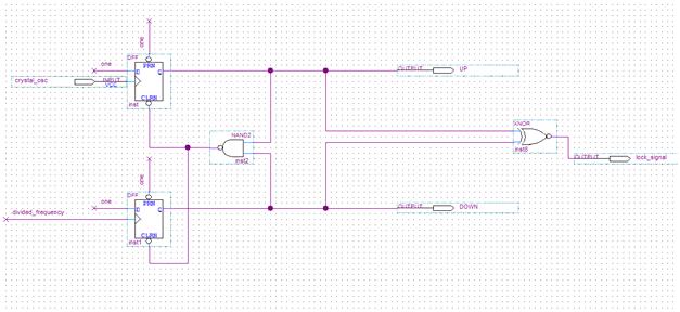
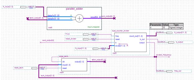
Our digital design for the phase-lock loop is composed by three parts: the Phase-frequency Divider (Figure 1), the dual modulus divider and the First Order Delta-Sigma modulator (Figure 2). The PFD consists of two D-Flip-flops and a NAND gate, with the XNOR logic to give a correct output for the lock signal of the loop. The Divider (Figure 2) is called dual_counter_divider, which implement a counter design and a dual modulus design. The Delta-Sigma modulator has two components: a parallel adder and a latch. These two components will function as a accumulator with a overflow signal output.
Figure 1. Block Diagram for PFD.
Figure 2. Block Diagram for Fractional-N divider.
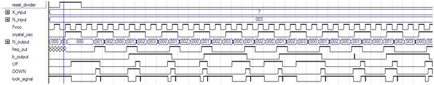
Figure 3. Simulation for Digital Fractional-N with Phase-Frequency Detector
In Figure 3, the simulation result of our Digital Fractional-N Frequency Synthesizer using PFD is shown to demonstrate the function of this design. Input signals include the reset_divider, K_input, N_input, Fvco, and F_ref, which can be found from the top of the figure. The output includes, the freq_out, b_output, UP, DOWN, and lock_signal. The schematic for this design is shown in Figure 1 and Figure 2.
Firstly, the input of the dividers are set as following: N value is 3 and K value is 7, the divider will divide the input high-frequency signal received from the VCO to a lower frequency by 3in the time average. The N_output indicates the output from the counter. The delta-sigma modulator controls the b_output signal by accumulating from 0 to 15, using the freq_out as reference clock. The b_ouput remains low for 9 cycles, and goes high for the other 7 cycles in a period of 24 cycles. It will ensure the divider works at N equal to 3 for the 7 cycles, and operates at N equalt to 4 for the remaining period. As the N_output signal shows, the counter in the divider counts from 0 to 2 in the beginning; when the b_output is high, the counter counts from 0 to 3. In the end, the output frequency from the divider is shown as freq_out. As a result, the output frequency operates at the rate of Fvco/3
in time average. The UP and DOWN signal will be connect to the charge pump. The lock_signal should be high only when both the UP and DOWN signals are high or low. When the lock_signal is 1 for a period longer than the loop lock time, the PLL is in the lock state. However, in this simulation the system is not locked because the comparison between the reference frequency (crystal_osc) and the divided frequency (freq_out) shows that these two signals are not in sync.